


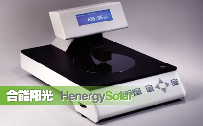
Products Brief:
Manual, non-contact measurement of wafer thickness, TTV and bow. Portable and easy to set-up, it measures all wafer materials including Silicon, Gallium-Arsenide, Indium-Phosphide and wafers mounted to sapphire or tape.

Product's Feature
■ Non-contact measurement
■ Material:Si, GaAs, InP, Ge, etc.
■Thickness and TTV values are obtained by placing the wafer between non-contact capacitance probes.
■Thickness and TTV values are indicated on the high resolution LCD display.
■Provides High Performance at Low Cost.
■Menu-driven for Fast, Easy Setup.
■On-board Microprocessor for Accurate, Repeatable Measurements.
■Teflon Wafer Stage for Easy, Non-abrasive Positioning.
Technique Specification
■ Wafer Size: 50mm-300mm.
■ Thickness range: 0-1000 um
■ Thickness accuracy: + /-0.25um
■ TTV Measurement accuracy: + /-0.05um
■ Bow range: + /-500um [+ /-850um]
■ Bow accuracy: + /-2.0um
Application
■Slicing
■Saw set-up
■Thickness
■TTV
■Degradation monitoring
■Wire guide re-grooving
■Blade replacement
■Lap/etch and polishing
■Process monitoring
■Thickness
■TTV
■Material removal
■Bow
■Warp
■Flatness
■Backgrind
■Removal rate
■Final Inspection
■Lot sampling
■Final thickness
Typical Customer:
American,Europe and Asia and so on.